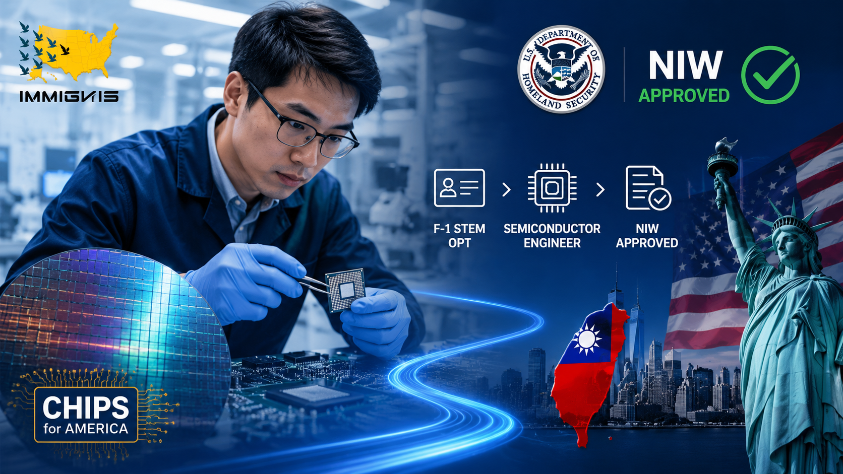
EB-2 NIW semiconductor engineer: An anonymized success story showing how a yield-enhancement and defect-reduction engineer used EB-2 NIW, premium processing, and an adjustment-of-status/EAD strategy when the H-1B lottery did not provide a solution.
Approval snapshot
| Nationality / location | Taiwanese national working in the United States on F-1 STEM OPT |
| Field | Semiconductor process engineering, yield enhancement, and defect reduction in chip fabrication |
| Career stage | Approximately six years of research and industry experience; rising senior engineer |
| Initial issue | STEM OPT window narrowing; H-1B lottery had not provided a solution |
| Pathway | EB-2 NIW with adjustment-of-status, EAD, and advance-parole strategy while the priority date was current |
| Engagement | Approximately nine months with a compressed build and filing sequence |
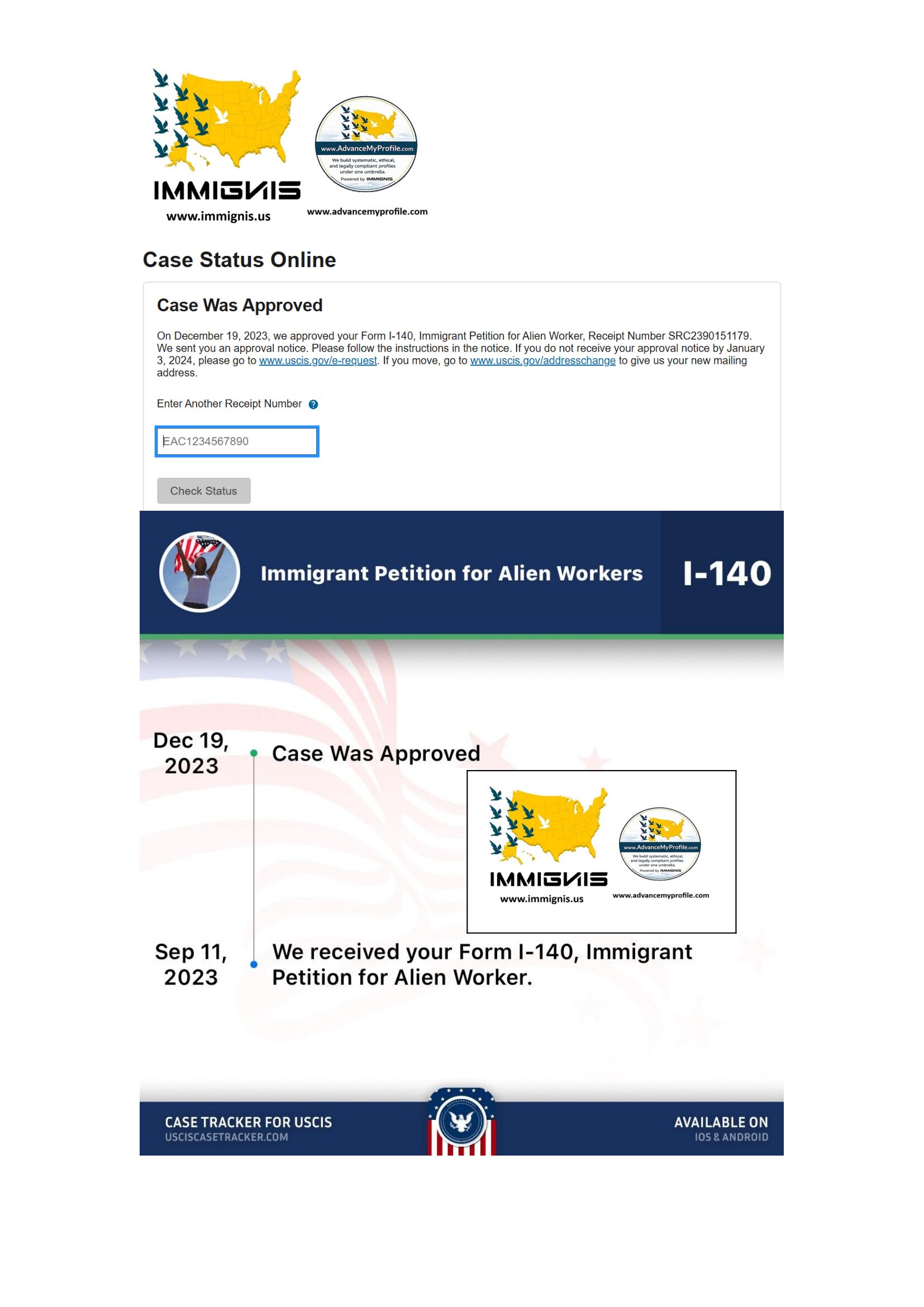
| Result | I-140 approved without RFE; I-485/EAD/AP strategy filed while the priority date was current; EAD issued |
The result: NIW approval and an EAD bridge before the OPT clock ran out
The case succeeded because it was built as both an immigration petition and a timing strategy. The I-140 was approved without a Request for Evidence. Because Taiwan’s EB-2 priority-date position was current at the relevant time, the adjustment-of-status package moved forward with the I-485, EAD, and advance-parole filings. After USCIS processing, the EAD was issued, giving the client work authorization independent of STEM OPT while the adjustment case continued.
This distinction mattered. The NIW approval created the foundation. The adjustment filing created the pending permanent-residence path. The EAD created the work-authorization bridge. The case worked because all three parts were planned together from the beginning.
The national problem: domestic chip manufacturing needs engineers who improve yield
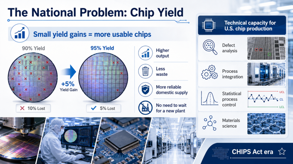
The client’s work addressed one of the most important bottlenecks in semiconductor manufacturing: yield. In a fabrication environment, yield determines how many usable chips come out of each wafer. Even a small improvement can increase output, reduce waste, and help a domestic fabrication facility deliver reliable supply without waiting for a new plant to be built.
His expertise sat at the intersection of materials science, process integration, equipment behavior, statistical process control, and defect analysis. He studied microscopic failures, identified where they entered the fabrication process, and helped develop process adjustments that reduced recurring defects. Under the CHIPS and Science Act environment, this was not ordinary manufacturing support. It was technical capacity directly tied to U.S. domestic chip production.
The client’s starting point
He was already doing valuable semiconductor engineering work in the United States, but his immigration position was fragile. He was on F-1 STEM OPT, and the H-1B lottery had not created a stable path. The risk was practical: if the work-authorization window closed, the United States could lose a process engineer working in the exact field federal policy was trying to strengthen.
The case could not be rushed, but it also could not be allowed to drift. The profile-building plan had to be selective, fast, and aligned with both the NIW legal standard and the adjustment-of-status timeline.
The proposed endeavor |EB-2 NIW semiconductor engineer
| “To develop and implement advanced yield-enhancement and defect-reduction processes for semiconductor fabrication - strengthening the technical capacity of U.S. domestic chip manufacturing facilities and supporting the manufacturing excellence goals of the CHIPS and Science Act.” |
The endeavor did not rely on the general importance of the semiconductor industry. It identified the specific mechanism: yield enhancement and defect reduction. It identified the sector: semiconductor fabrication. It tied the work to a federal commitment: domestic semiconductor manufacturing under the CHIPS and Science Act. That kept the national-importance argument concrete and officer-friendly.
What AdvanceMyProfile and Immignis built
- Focused publication record: Additional technical writing was aligned to yield improvement, defect characterization, process control, and advanced fabrication conditions rather than unrelated semiconductor topics.
- Original-contribution evidence: A patent filing on defect inspection and root-cause identification created a dated record of technical contribution connected to the client’s industry work.
- Senior professional recognition: A peer-reviewed senior membership route was pursued in a relevant semiconductor or electrical-engineering professional body, avoiding basic pay-to-join memberships.
- Industry and policy visibility: Expert commentary was placed around yield improvement, defect reduction, domestic fab readiness, and the engineering challenge behind CHIPS Act implementation.
- Targeted white paper: A concise white paper on yield improvement as a bottleneck in domestic semiconductor manufacturing was shared with relevant semiconductor, engineering, and technology-policy audiences.
- Independent expert letters: U.S.-connected experts addressed his process-characterization methods, defect-reduction relevance, and why yield expertise mattered to CHIPS Act manufacturing goals.
- Filing sequence: The I-140, premium-processing decision, I-485, EAD, advance-parole materials, and OPT compliance plan were mapped as one coordinated strategy.
How the evidence supported the Dhanasar framework
Substantial merit and national importance: The petition connected semiconductor yield improvement to domestic chip manufacturing capacity, production reliability, supply-chain resilience, and the CHIPS and Science Act’s manufacturing objectives.
Well-positioned to advance the endeavor: The record showed focused education, industry process-engineering experience, publications, citations, a patent filing, senior recognition, expert commentary, and independent letters tied directly to defect reduction and yield improvement.
Benefit of waiving the job-offer and labor-certification requirement: The filing explained why retaining specialized semiconductor process talent served a national manufacturing priority, especially where the H-1B lottery could otherwise interrupt the continued contribution of an engineer already working in the United States.
The filing and approval
Premium processing was used because timing was central to the strategy. Premium processing did not guarantee approval; it only guaranteed faster USCIS action. In an OPT-sensitive case, that predictability mattered. USCIS approved the I-140 without a Request for Evidence.
Because the priority date was current at the relevant time, the adjustment-of-status strategy proceeded with the I-485, EAD, and advance-parole filings. The EAD was later issued, giving the client an independent work-authorization bridge while the adjustment case continued. The green-card process was not instantly finished, but the immediate work-authorization crisis was controlled.
What changed after the approval
The approval stabilized his position in the United States and changed how his employer could plan around him. A process engineer who might have been forced out by OPT expiration and H-1B uncertainty became a long-term technical asset. His patent filing and public profile also made his expertise easier to explain internally and to external collaborators.
He later received broader responsibility in defect-reduction projects connected to domestic manufacturing expansion, improved compensation, and moved toward a more senior process-integration role. A second domestic fab project also expressed interest in his yield-improvement experience. The immigration strategy did not create his expertise; it made that expertise visible, stable, and usable in the U.S. semiconductor ecosystem.
What this case teaches
- OPT cases require calendar discipline. A strong NIW may not solve the problem if the filing sequence does not protect work authorization.
- Taiwan chargeability can materially change strategy when EB-2 is current. The visa bulletin must still be checked at filing, but current chargeability can make adjustment filing possible.
- The CHIPS Act is useful only when the petitioner’s work genuinely fits the manufacturing problem. The petition must identify the technical bottleneck, not merely use the word semiconductor.
- Premium processing gives timing predictability, not guaranteed approval. In deadline-sensitive cases, that predictability can be essential.
- A patent filing, focused publications, industry commentary, white paper circulation, and independent letters work best when every item supports the same technical story.
- Ethical profile building documents real expertise. It does not manufacture a false profile or force unrelated evidence into the record.
If you are on F-1 OPT or STEM OPT and the H-1B lottery has not provided a solution, your strategy should begin with chargeability, timing, and the real strength of your NIW record. The right question is not only whether you can file an I-140. It is whether the I-140, adjustment filing, EAD plan, and work-authorization timeline can be coordinated lawfully and credibly.
See how Immignis builds NIW timing strategies that protect your work authorization.