Key facts at a glance
| Outcome | EB-1A approval for a Japanese semiconductor lithography engineer working at a Japan based chip-equipment company. |
| Approval date | Approved on September 4, 2024. |
| Field niche | Lithography process optimization for advanced-node chips, with a focus on overlay, focus behavior, metrology feedback, and stable process performance. |
| Starting problem | His role was technically strong but employer-sensitive. Much of the visible record described company equipment and customer processes, making his individual process-engineering contribution hard to isolate. |
| Path used | Ethical EB-1A profile building through non-confidential publications, process-improvement documentation, patent evidence, semiconductor conference roles, technical commentary, peer review, selective professional membership, critical-role evidence, and independent expert letters. |
| USCIS EB-1A criteria activated | Original contributions, scholarly articles, published material, judging, and leading or critical role. Patent evidence strengthened the original-contribution record. |
USCIS approved his Form I-140 on September 4, 2024.
The story had started with two wafer layers that looked acceptable when reviewed separately. EB-1A semiconductor lithography engineer started here.
Placed on top of each other, the problem appeared. The printed features were not lining up as expected across the wafer. A process engineer could describe the symptom in one sentence. Finding the source meant reading metrology data, focus behavior, process history, and the interaction between the lithography system and the wider manufacturing flow.
He was a Japanese semiconductor lithography engineer working for a chip equipment company in Japan. Colleagues knew him as the person called when a process window began to tighten or a patterning problem refused to fit the first explanation. His EB-1A record showed far more about the employer’s technology than about him.
The equipment belonged to the company. The process judgment had to be traced to the engineer.
Semiconductor equipment companies protect technical information for good reason. Tool architecture, customer data, process recipes, correction methods, and performance details can be commercially sensitive.
An engineer may spend years improving advanced manufacturing processes while the public record contains a job title, a few patents, and conference activity described at a high level. EB-1A is a self-petition immigrant classification for individuals who can demonstrate extraordinary ability through sustained national or international acclaim and recognition of achievements in their field.
The Form I-140 petition needed evidence showing what he had contributed, how other specialists recognized his expertise, and why the record placed him at the top level of a defined field.
The field became lithography process optimization for advanced-node chips
Lithography builds chip patterns layer by layer on a wafer. The pattern must be printed with extraordinary precision, and later layers have to align with structures already created.
The profile team traced repeated involvement in overlay, focus behavior, process window analysis, metrology feedback, and the investigation of pattern variation across wafers and production conditions. The professional subject was his process expertise: interpreting patterning data, isolating likely causes, and guiding process adjustments when advanced node manufacturing tolerances leave little room for drift.
What did USCIS need to see in a lithography process optimization case?
The petition first presented evidence under the applicable USCIS EB-1A criteria. At final merits, the officer could examine the quality of that evidence and whether the whole record showed sustained acclaim and top level expertise.
For original contributions, the file had to identify process improvement work, analytical methods, technical concepts, or documented problem solving linked to him. Company ownership of the tool did not establish his individual contribution.
Scholarly articles needed to concern lithography and process control. Published material required independent coverage about him or his expertise. Peer review and semiconductor conference evaluation roles supported judging only where he actually assessed the work of others. The leading or critical role evidence focused on the technical decisions, process escalations, and advanced manufacturing work that depended on his judgment.
Process improvement documentation turned invisible engineering work into evidence
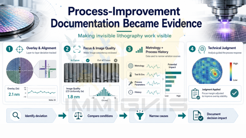
Project summaries, non-confidential technical notes, role descriptions, and process-improvement documentation were organized around the lithography problems he had handled. The team looked for the point where his analysis entered the process and the decision that followed.
One group of records concerned layer to layer alignment and overlay behavior. Another concerned focus and image quality across the wafer. Other material showed how metrology results and process history were used to narrow the source of variation.
The petition did not publish customer recipes, proprietary correction algorithms, or protected tool settings. The evidence showed the engineering sequence: identify the deviation, compare data across relevant conditions, narrow likely causes, and document where his technical judgment influenced the process response.
The publications were built around open lithography problems
With domain support, he developed focused papers on lithography process control, overlay behavior, focus variation, metrology feedback, and the interpretation of patterning data in advanced semiconductor manufacturing.
The papers used non-confidential scientific questions. Employer-owned system details and customer-specific process information stayed outside the manuscripts.
The subjects came from real process questions: whether an apparent patterning problem was local, systematic, wafer dependent, process dependent, or connected to another manufacturing step. His papers showed how he approached those questions without exposing the protected technology behind a commercial platform.
Semiconductor engineers often have years of process expertise hidden inside confidential programs, customer support, and employer-owned technology. A free EB-1A profile assessment can identify which contributions are attributable to you and where authorship, judging, public recognition, or independent evidence can be built safely.
Patent evidence helped show inventorship, but the case still had to prove significance
Where the available patent materials identified him as an inventor or contributor, the petition used the public record to trace his role in a specific process or technical idea.
Patent evidence supported the original-contribution argument. Patents are not a separate EB-1A regulatory criterion. The wider evidence still had to explain why the technical concept mattered. Process documentation, publications, critical role records, and independent semiconductor experts supplied that context.
Semiconductor conference roles were documented by what he actually evaluated
He served in technical roles connected to semiconductor and process-engineering programs. Advance My Profile separated presentations, committee service, abstract review, and other evaluation work so each activity was described accurately.
Where he reviewed technical submissions or helped assess research proposed for a conference program, the file documented the judging function. A conference title alone was not enough. The evidence identified the type of work submitted by others and the part he played in evaluating it.
Technical commentary made lithography understandable without revealing a process recipe
Industry and semiconductor audiences could discuss why chip patterns are built layer by layer, why alignment between layers matters, and why focus and process variation become difficult as manufacturing tolerances tighten.
He explained how metrology gives engineers information about what was actually printed on a wafer and why process optimization depends on reading patterns across multiple data sources.
The commentary stayed away from customer problems, internal tool specifications, and proprietary correction strategies. Independent coverage identified him with lithography control and advanced-node manufacturing, the same subject visible in his papers and conference work.
Selective membership and peer review created recognition outside the employer
Professional organizations can offer open membership, advanced grades, or technically selective recognition. The petition used membership evidence only where the admission standards and expert assessment supported it.
Peer review developed separately. Journals and technical venues asked him to assess research in lithography, process control, semiconductor manufacturing, and related fields. The record documented genuine review work and kept weak mass invitations out of the case.
Independent experts separated his expertise from employer-owned technology
Independent experts explained the process problem first. Chip patterns are formed layer by layer, and manufacturing teams use metrology and process data to monitor alignment, focus, and pattern quality. Small process errors can become defects or yield problems.
Advance My Profile prepared evidence-based drafts for expert review, and referees could revise the language and sign only what they considered accurate. The letters answered the central question: what belonged to the engineer when the technology platform belonged to the employer?
How the USCIS EB-1A criteria came together in this semiconductor case
Original contributions: Process-improvement documentation, patent evidence, technical methods, critical project records, and independent semiconductor letters explained his individual contribution to lithography process optimization and its significance.
Scholarly articles: Focused papers connected his authorship to lithography process control, overlay behavior, focus variation, metrology feedback, and advanced semiconductor manufacturing.
Published material: Independent semiconductor and industry coverage discussed him or his expertise in lithography optimization, patterning control, and advanced-node process challenges.
Judging the work of others: Peer-review records and documented technical evaluation roles in semiconductor conferences showed genuine assessment of research and technical submissions by other specialists.
Leading or critical role: Employer and project evidence showed why significant advanced manufacturing and lithography process work relied on his technical analysis, process judgment, and escalation responsibility.
Process documents showed where his judgment entered manufacturing problems. Papers made the technical subject public. Patent evidence traced inventorship. Conference evaluation and peer review showed professional trust. Media, role evidence, and independent letters showed recognition beyond one employer.
Approval came on September 4, 2024
The approved EB-1A petition gave him a self-petition immigration path without employer sponsorship or labor certification. The filing established a priority date for the immigrant petition, while later permanent-residence timing can depend on visa availability and the applicant’s next immigration step.
If your semiconductor career is hidden behind a famous tool, fab, or employer
A tool may belong to the company, a process recipe to the customer, and a production line may involve hundreds of engineers. Your EB-1A record still needs to identify the technical problems, decisions, and recognition that can be traced to you.
Build public authorship around scientific questions you can discuss. Document process improvements with non-confidential evidence. Use patent records according to their status. Accept genuine review and conference evaluation work. Ask independent experts to discuss contributions they can evaluate.
For semiconductor professionals comparing EB-1A with EB-2 NIW, the legal questions are different. EB-1A centers on extraordinary ability and sustained acclaim. EB-2 NIW examines EB-2 eligibility and a proposed endeavor under the national interest waiver framework.
FAQs
Can confidential semiconductor process work support an EB-1A case?
Yes. The petition still needs verifiable evidence of the engineer’s individual contribution and recognition, but protected process recipes or customer data do not have to be disclosed carelessly. Non-confidential process documentation, public patents, focused publications, judging, professional roles, and independent expert evidence can help when they are tied to the applicant’s real work.
How can a lithography engineer prove process optimization without revealing a customer recipe?
The record can identify the process problem, the applicant’s analytical role, the type of data reviewed, the engineering sequence used to narrow causes, and the documented response without publishing proprietary parameter values. Public technical writing and independent experts can then explain why the method matters in lithography process control.
Does a semiconductor patent count as a separate EB-1A criterion?
No. Patent evidence is not a separate EB-1A regulatory criterion. It may support an original-contribution argument by documenting inventorship and a technical concept, while the wider record still needs to show the significance of the contribution.
Can a semiconductor conference committee role count as judging for EB-1A?
It can when the engineer actually evaluates the work of others, such as abstracts, papers, technical proposals, or submitted research. The petition should document the evaluation function. Speaking, organizing, and attending are separate activities unless the role also included judging.
Should a semiconductor engineer consider EB-1A or EB-2 NIW?
The categories apply different legal standards. EB-1A focuses on extraordinary ability, sustained acclaim, and recognition in the field. EB-2 NIW requires EB-2 eligibility and a proposed endeavor that satisfies the national-interest-waiver framework. A semiconductor career may contain evidence relevant to both, but the petition strategy should match the chosen standard.
Do I need a PhD to pursue EB-1A as a semiconductor lithography engineer?
No specific PhD is required for EB-1A extraordinary ability. A lithography engineer may rely on applicable evidence such as original contributions, scholarly authorship, judging, published material, leading or critical roles, and sustained independent recognition. Education can support the background, but the full extraordinary-ability record is what USCIS evaluates.
Build an EB-1A success story around the process expertise that belongs to you
If you work in semiconductor lithography, process integration, metrology, wafer patterning, advanced-node manufacturing, or chip equipment, your strongest work may sit inside employer and customer systems. Immignis and Advance My Profile help identify a defensible technical niche, document individual process contribution, build credible recognition, and prepare an EB-1A record without turning protected technology into public content.