Key facts at a glance
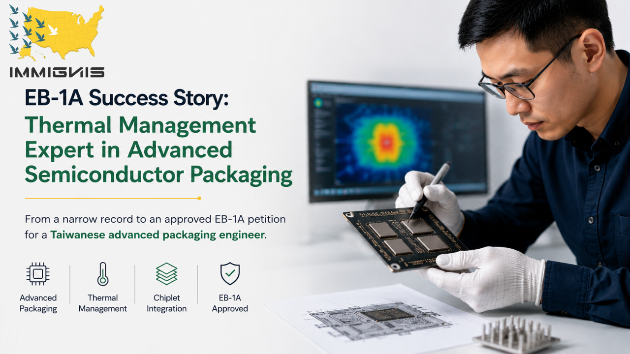
| Outcome | EB-1A approval for a Taiwanese advanced packaging engineer working at a U.S. based semiconductor manufacturer. |
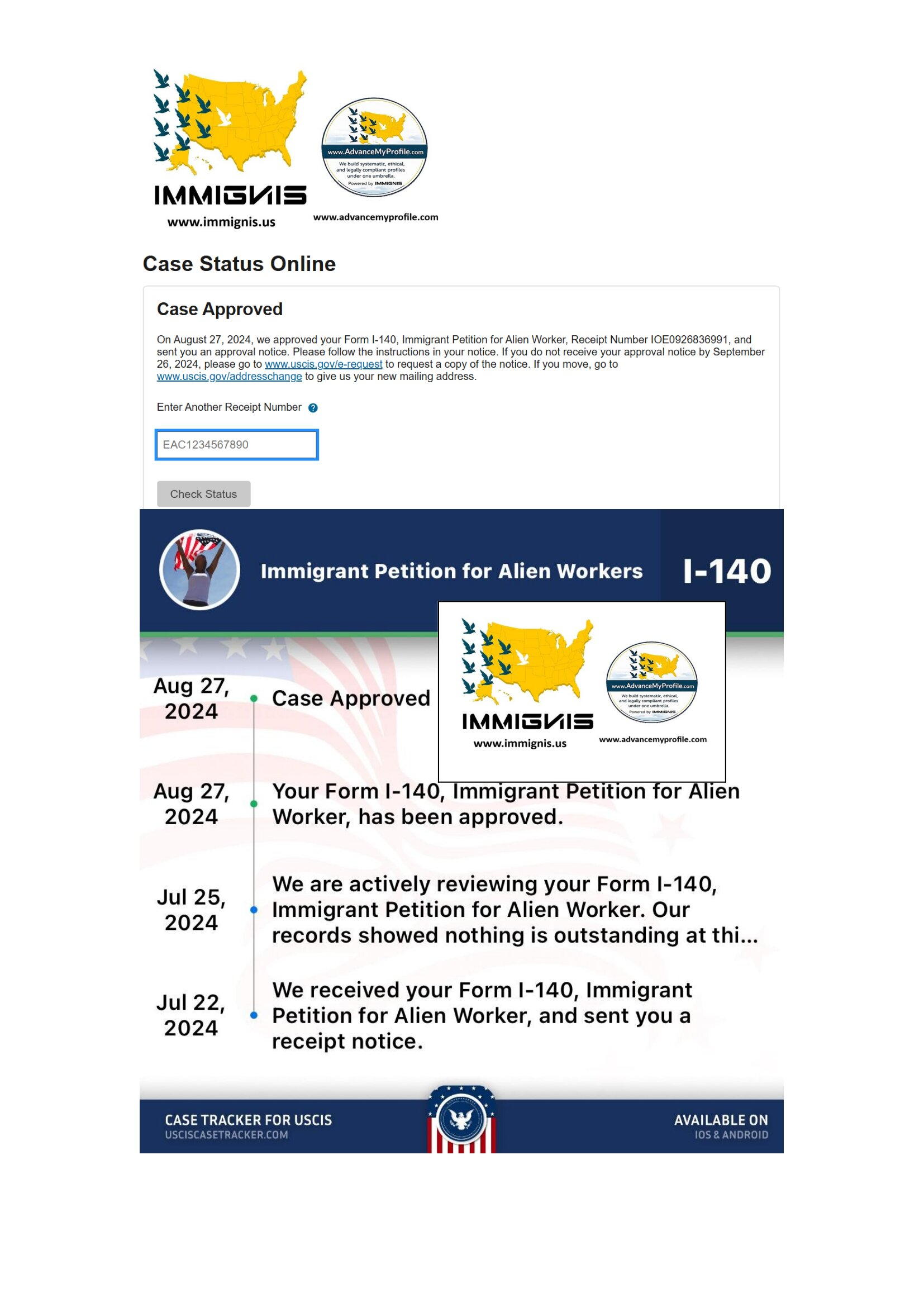
| Approval date | Approved on August 27, 2024. |
| Field niche | Thermal management in chiplet and advanced semiconductor packaging systems, with a focus on heat paths, package integration, and performance stability. |
| Starting problem | The technical work was high value, but the public record was narrow. Most evidence described internal package programs and employer-owned technology instead of his individual packaging expertise. |
| Path used | Ethical EB-1A profile building through focused publications, patent filing, non-confidential process and thermal-analysis evidence, an advanced-packaging white paper, conference talks, peer review, trade media coverage, selective membership, and independent letters from packaging experts. |
| USCIS EB-1A criteria activated | Scholarly articles, original contributions, published material, judging, and memberships. Patent evidence strengthened the original contribution record. |
USCIS approved his Form I-140 on August 27, 2024.
The problem that opened his profile review was smaller than a fingernail. EB-1A for Semiconductor Engineers requires strong evidence of extraordinary ability. Several chiplets were doing different kinds of work inside one advanced package. On a diagram, the arrangement looked compact and efficient. Under load, the thermal picture was less tidy. One region was carrying heat differently from the rest of the package.
He was a Taiwanese advanced packaging engineer working at a U.S. based semiconductor manufacturer. His work sat where chip architecture met physical reality: dies, interconnects, package materials, heat paths, assembly constraints, and the question of whether a high performance device could keep operating inside its intended thermal limits.
A narrow public record can hide high value semiconductor work
Package programs have schedules, design reviews, qualification steps, and team owned records. By the time a device reaches customers, the engineer’s personal contribution may be buried under the company brand.
The EB-1A green card is a self-petition immigrant classification for individuals who can demonstrate extraordinary ability through sustained national or international acclaim and recognized achievements in their field.
USCIS needed evidence of his own standing in advanced packaging. The employer explained the environment, while the petition had to prove his individual contributions and recognition.
Advance My Profile, powered by Immignis, reviewed his work with legal strategists and semiconductor packaging specialists and narrowed the profile to thermal management in chiplet and advanced packaging systems.
His field began with a simple question: where does the heat go?
Chiplets allow different functional dies to be integrated within a package. Heat is generated in specific locations, travels through several materials and interfaces, and can affect nearby components.
The evidence showed recurring analysis of local heat concentration, die placement, package interfaces, thermal resistance, materials, cooling assumptions, and sustained device performance.
A package can meet an electrical objective and still create a difficult thermal condition, while a thermal solution may affect mechanical, manufacturing, or integration choices. His contribution was not described as owning an entire AI chip or packaging platform. The case focused on the thermal-management methods and integration judgment that could be traced to him.
What did USCIS need to see in an advanced packaging EB-1A case?
For original contributions, the petition had to identify his technical methods, thermal-analysis work, package concepts, or process improvements and then show why they had major significance in advanced packaging. Internal program importance alone was not enough.
Scholarly articles needed to concern chiplet packaging, heat transfer, package integration, or allied semiconductor subjects. Published material required independent coverage about him or his expertise. Peer review supported judging when he actually evaluated research by other specialists.
The memberships criterion required selective admission or elevation standards tied to achievement and expert assessment. Open professional enrollment was kept separate.
Patent evidence helped trace inventor ship and technical concepts. It supported the original contribution record; patents are not a separate USCIS EB-1A regulatory criterion.
At final merits, the papers, technical record, patent evidence, judging, membership, media, and independent letters had to describe the same packaging specialist.
The internal engineering record was rebuilt around thermal decisions
Project summaries, role records, process-improvement documents, public invention materials, and safe package descriptions were grouped by engineering question instead of product name.
Where was the heat concentrated? Which path carried it away? What thermal assumption was being tested? Which interface or material mattered, and what decision changed after his analysis?
The evidence covered hotspot behavior, thermal spreading, package interfaces, materials, and the point where thermal analysis entered integration or process decisions. Protected product data, customer identities, and internal package details stayed out of the public record.
The publications connected chiplet performance to package level thermal behavior
With domain support, he developed papers on chiplet thermal management, local heat density, package heat paths, interface effects, and thermal analysis in package integration.
The papers stayed with scientific and engineering questions that could be discussed publicly. One paper examined why average package temperature can hide a local hotspot. Another studied heat flow through interfaces when multiple dies have different power profiles. These subjects came directly from the type of decisions he had handled in semiconductor programs.
Semiconductor packaging professionals often have years of high value work hidden inside confidential integration programs. A free EB-1A profile assessment can identify which methods are attributable to you and where authorship, judging, membership, media, or independent recognition still needs development.
A patent filing helped document the technical concept
Where the filing identified him as an inventor, the public record connected him to a packaging or thermal management concept. Technical evidence and independent analysis explained the problem it addressed.
The filing itself did not establish major significance. Significance came from the wider record: the thermal problem, his engineering work, the concept’s relevance to package integration, and explanations from packaging specialists.
The advanced packaging white paper was written for AI-chip and manufacturing audiences
The white paper addressed the thermal limits that advanced packaging can create for high performance computing and AI-oriented semiconductor systems. Its audience included packaging engineers, semiconductor manufacturers, technical suppliers, and professionals interested in domestic chip production.
The paper organized the subject around heterogeneous integration, chiplet heat density, thermal interfaces, package materials, cooling assumptions, and validation.
The paper treated packaging as one part of a wider performance system that also includes power, architecture, interconnects, software, and cooling.
The white paper gave the client a public document that connected his packaging specialty to the performance and manufacturability of advanced chips.
Conference talks gave other packaging engineers a chance to challenge the method
His conference presentations focused on package integration and thermal analysis. He discussed hotspot identification, thermal paths, die placement, interface effects, and the difference between a package average temperature and a local condition near a high-power region.
Engineers asked about measurement, modeling assumptions, material selection, and the point at which a thermal issue should change a package decision. Judging evidence was handled separately through peer review, where he evaluated research submitted by other specialists.
Peer review showed that the field trusted his technical assessment
Journals and technical venues invited him to review work in semiconductor packaging, thermal management, electronics cooling, materials, and related engineering areas.
The file documented genuine review assignments and completed activity where available. The reviewed research required judgment about methods, thermal assumptions, and whether conclusions followed from the evidence.
Weak mass invitations were not used to create a judging count. For USCIS, the peer-review record showed actual evaluation of other specialists’ work in the same or an allied field.
Trade media made advanced packaging understandable without turning him into a general chip commentator
Trade publications discussed chiplets, hotspot behavior, thermal interfaces, and why package design matters as computing systems become denser.
He explained that different dies may have different power profiles and that heat does not distribute evenly simply because a package looks symmetrical. The commentary stayed away from unreleased products, internal package roadmaps, and customer programs.
Selective membership created recognition outside one semiconductor manufacturer
Advance My Profile reviewed admission or elevation standards for professional organizations connected to semiconductor packaging and electronics.
The petition used the criterion only where the membership grade relied on relevant achievements and evaluation by recognized experts. The file included the applicable advancement requirements and evidence showing how his professional record was assessed.
Independent packaging experts could finally point to his contribution
Independent experts began with the engineering problem. Chiplets and heterogeneous packages place several functional dies into a tightly integrated system, where local power density can affect package and cooling decisions. They discussed his papers, patent evidence, non-confidential thermal analysis work, and conference record.
The letters explained why hotspot analysis, package heat paths, interface behavior, and thermal validation matter for demanding workloads.
How the USCIS EB-1A criteria came together in this advanced packaging case
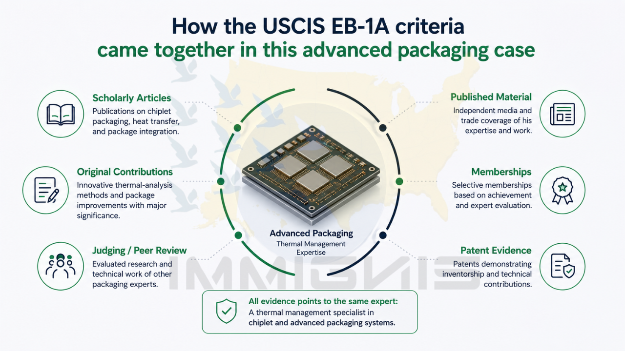
Scholarly articles: Focused papers connected his authorship to chiplet thermal management, package heat paths, hotspot behavior, interface effects, and advanced semiconductor integration.
Original contributions: Non-confidential thermal analysis evidence, process-improvement documentation, patent materials, publications, and independent packaging letters explained his individual contribution and its significance.
Published material: Independent semiconductor and trade coverage discussed him or his expertise in advanced packaging, chiplets, and thermal management.
Judging the work of others: Peer-review records documented genuine evaluation of research by other specialists in semiconductor packaging, thermal management, materials, and allied fields.
Memberships: Selective professional membership evidence included the relevant admission or elevation standards and documentation of expert assessment based on achievement.
The papers made the thermal questions public. Patent evidence traced a technical concept. The white paper connected packaging to advanced chip performance and manufacturing. Peer review and selective membership showed outside assessment. Conference talks, trade media, and independent letters carried the same specialty beyond internal programs.
USCIS could see the heat problem, the method, and the engineer responsible for part of the solution.
Approval came on August 27, 2024
The approved EB-1A petition gave him a self-petition immigration path without employer sponsorship or labor certification. The filing established a priority date for the immigrant petition, while later permanent residence timing can depend on visa availability and the applicant’s next immigration step.
If your packaging work is important but almost nothing is public
Maybe it is hotspot behavior, warpage, interconnect reliability, thermal interfaces, package materials, power delivery, or manufacturing yield. Define the area closely enough that another packaging engineer would recognize your work.
Document non-confidential methods, process improvements, and decisions attributable to you. Publish around open engineering questions. Use patents according to their real status. Build judging through genuine peer review and rely on membership only when the admission or elevation standard supports the criterion.
Do not create a profile from fake recognition, junk publications, or technical claims you would hesitate to defend in a packaging review. USCIS scrutiny matters, and your professional reputation lasts much longer.
Build evidence you will still be proud to show another engineer years after the immigration case is finished.
FAQs
Why does thermal management matter in chiplet and advanced packaging systems?
Chiplets and heterogeneous packages can place several dies with different power profiles into a compact system. Heat may concentrate in local regions and move through package materials and interfaces in uneven ways. Thermal behavior can affect design, cooling, reliability, and the conditions under which a device can sustain performance.
Can confidential semiconductor packaging work support an EB-1A original-contribution claim?
Yes, when the applicant’s individual contribution can be identified through verifiable, lawfully usable evidence. Non-confidential process records, public patent materials, technical publications, documented methods, and independent expert analysis can help explain the work without disclosing protected package designs or customer data.
Does an advanced packaging patent count as a separate EB-1A criterion?
No. Patents are not a separate EB-1A regulatory criterion. Patent evidence may help document inventorship and support an original-contribution argument, while the petition still needs evidence explaining the significance of the technical contribution.
Can peer review count as judging for a semiconductor packaging engineer?
Genuine peer review can support the judging criterion when the engineer actually evaluates research by other specialists in the same or an allied field. The petition should document the invitation and review activity, and the technical subject should fit the applicant’s expertise.
How can advanced packaging expertise relate to AI-chip performance?
AI and high-performance computing devices can involve dense integration and high power levels, so package-level heat paths and local hotspots can become important engineering constraints. Advanced packaging engineers study materials, interfaces, die arrangement, thermal resistance, and cooling assumptions as part of the wider system that supports sustained device operation.
Do I need a PhD to pursue EB-1A as an advanced packaging engineer?
No specific PhD is required for EB-1A extraordinary ability. A packaging engineer may rely on applicable evidence such as original contributions, scholarly authorship, judging, published material, qualifying memberships, and sustained independent recognition. USCIS evaluates the full extraordinary-ability record.
Build an EB-1A success story around the package-level problem you are known for solving
If you work in chiplets, semiconductor packaging, heterogeneous integration, electronics cooling, thermal management, or advanced manufacturing, your strongest technical contribution may still be hidden inside internal programs.
Immignis and Advance My Profile help identify a defensible technical niche, document individual methods, build credible field recognition, and prepare an EB-1A record around evidence you can verify and defend professionally.